Nexstrom · Singapore · Founded 2024
The wafer-scale 2D semiconductor platform for the next generation of AI chips.
We enable foundries to scale advanced nodes beyond silicon for ultra-low-power compute.
- Platform
- North Star™ cold-wall CVD (MOCVD)
- Material
- 2D TMDs: MoS₂, WSe₂
- Target format
- 300 mm (12-inch) wafers
- Capital raised
- US$15M
- Xora Innovation
- Foothill Ventures
- SEEDS (SG Growth Capital)
Backed by
The silicon limit
Shrinking silicon is running into physics.
- Gate control
- Off-state leakage
- Gate control
- As the channel gets shorter, the drain’s electric field reaches under the gate. The gate can no longer fully switch the transistor off.
- Leakage and heat
- Current that flows while a transistor is off wastes energy as heat. A chip has billions of transistors, so this adds up to a hard power limit.
- Thinner silicon, up to a point
- A thinner silicon body gives the gate back some control. At a few nanometres, rough surfaces start to scatter the current instead.
- Atomically thin channels
- A 2D TMD monolayer is under a nanometre thick, which gives the gate strong electrostatic control at extreme dimensions. Its ideal surface has no dangling bonds, which helps carriers keep moving well at that thickness.
2D transistors are on the IRDS roadmap for the beyond-1 nm logic node because of their “ultrathin thickness and defect-free surfaces”. Nature 655, 350 (2026)
Why 2D TMDs
Two materials, both polarities.
A transition-metal dichalcogenide monolayer is a sheet of metal atoms between two sheets of chalcogen atoms. CMOS logic needs both n-type and p-type transistors, and the TMD family covers both.
- MoS₂n-type channelMolybdenum disulfideNanosheet FETs (VLSI 2026) · contact scaling (Nature 2026)
- WSe₂p-type channelTungsten diselenideSingle-orientation monolayers (ACS Nano 2026) · bilayer MOCVD (EDTM 2026)
- MoS₂ / WSe₂CFET logicStacked n- and p-channels2D CFET inverters; wafer-scale NAND/NOR gates (IEDM 2025)
| Material | Role | Peer-reviewed results |
|---|---|---|
| MoS₂Molybdenum disulfide | n-type channel | Nanosheet FETs (VLSI 2026) · contact scaling (Nature 2026) |
| WSe₂Tungsten diselenide | p-type channel | Single-orientation monolayers (ACS Nano 2026) · bilayer MOCVD (EDTM 2026) |
| MoS₂ / WSe₂Stacked n- and p-channels | CFET logic | 2D CFET inverters; wafer-scale NAND/NOR gates (IEDM 2025) |
North Star™ · the platform
Purpose-built for wafer-scale 2D TMD growth.
North Star grows transition-metal dichalcogenide monolayers across full wafers, for integration into foundry device flows. The layer is meant to become the channel of each transistor, replacing silicon at the core of the device. Material that looks good in a lab sample is not the same as uniform, device-grade material across a production wafer. North Star is built for the second.
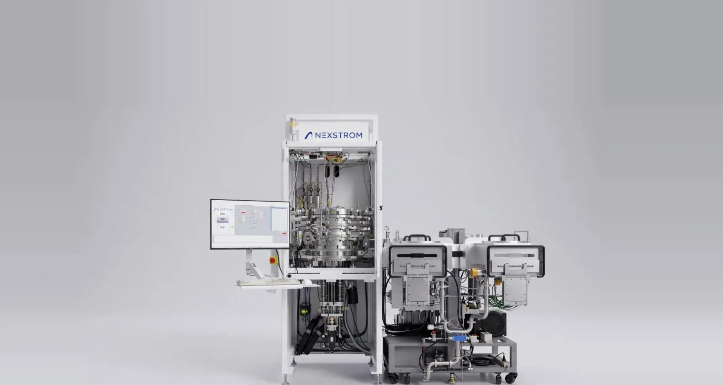
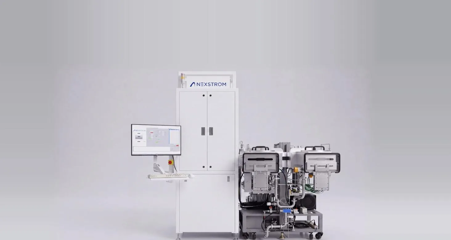
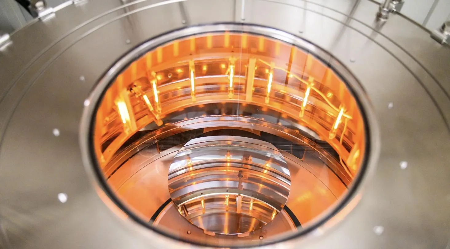
Precise vapor-phase delivery for stable chemistry and repeatable process windows.
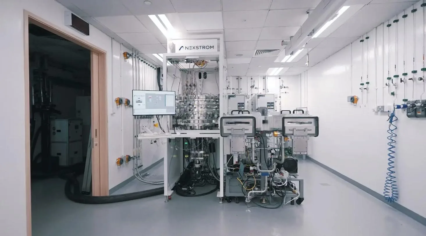
In the lab
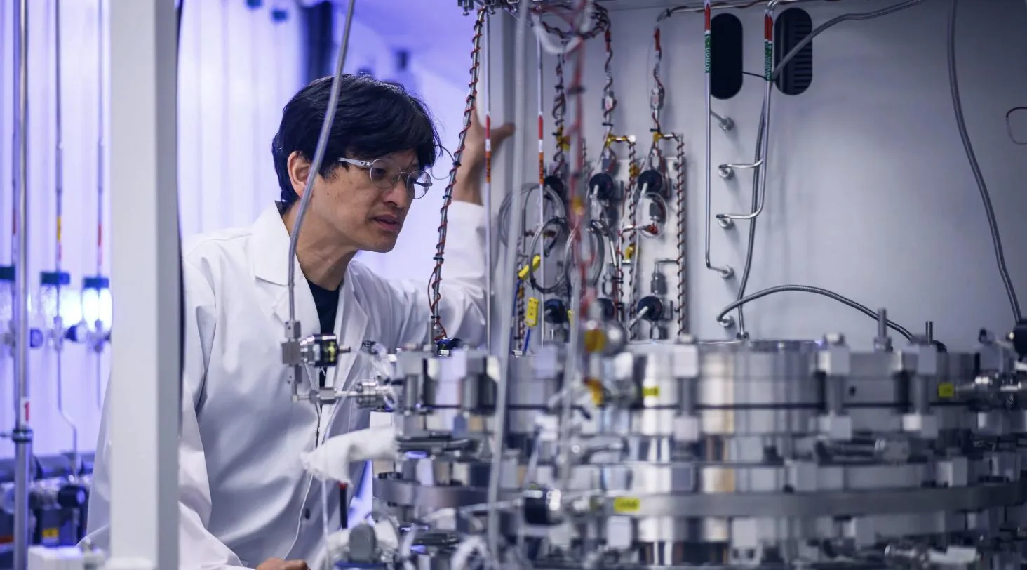
North Star in Nexstrom’s lab. The platform combines proprietary deposition hardware, process technology and wafer-scale 2D growth, and is designed to fit a foundry’s existing workflow.
Atomically thin.
Wafer scale.
A TMD monolayer is about 0.65 nm thick. A production wafer is 300 mm across, a ratio of roughly 460 million to one. Scale the wafer up to the width of Singapore (≈50 km) and the layer would be as thick as a sheet of paper.
- 2 inSystematic scale-up startAchieved
- 100 mmPilot → 100 mm, 2025Achieved
- 6 inReported Sep 2026Achieved
- 8 inTargeted end Oct 2026Targeted
- 12 inTarget format. 12-inch system installed; material results reportedCompany-reported
Scale-up path per nexstrom.com (2025: pilot → 100 mm) and CEO Phoebe Tan to TechCrunch, 22 Sep 2026: “systematically scaled from 2 inches to 6 inches… 8 inch by the end of October”, with “proven material results” on the newly installed 12-inch system.
Performance
Transistors built for the Angstrom era.
- Up to100×Lower defect density
Fewer micro-voids and interface flaws at the atomic scale, which matters for yield on 300 mm wafers.
Company-reported - Up to75%Less switching power
Stronger gate control and lower leakage, so more operations fit in the same energy budget.
Company-reported - Over2×Smaller gate length
Atomically thin channels let the gate shrink further while keeping control of the channel.
Company-reported
Peer-reviewed results from Nexstrom’s scientists and collaborators
- 98.44%single-orientation WSe₂ monolayer
Across a two-inch c-plane sapphire wafer. Prior p-type benchmarks were about 82–87%.
DemonstratedACS Nano · 2026 - ≈2.0 nmcarrier transfer length
Measured at the bismuth contact of a monolayer MoS₂ transistor by cross-sectional STM.
MeasuredNature · 2026 - 0.1–1 Vrail-to-rail 2D CFET inverters
Stacked n-MoS₂ / p-WSe₂ on single-crystal TiO₂ dielectric. The authors report record-low standby power.
DemonstratedIEDM · 2025 - 1 nmnode SRAM projection
TCAD extrapolation: 2D CFET SRAM exceeds Si-GAA projections in speed and energy.
ProjectedIEDM · 2025
From lab to fab
Moving fast, and clear about where we are.
- 2024AchievedInvestmentPlatform foundation
- Founded by Lance Li and Xora Innovation
- Validated a proprietary wafer-scale TMD growth platform for high-quality 2D semiconductors
- Established the core intellectual property and technology roadmap
- 2025AchievedBuildLab to fab scaling
- Advanced the MOCVD platform from pilot to 100 mm wafer scale
- Expanded IP to TMD epitaxial growth, transfer processes and device integration
- Demonstrated reproducible wafer-scale growth with high uniformity and process stability
- 2026Company-reportedScaleCommercial traction
- Commercial-grade TMD synthesis on 300 mm wafers
- Wafer samples delivered to industry partners within 18 months of launch
- 7 active patent families, including an issued US foundational patent
- US$15M raised, including a US$12M seed round and US$3M non-dilutive funds
- NextExpectedQualifyToward production
- 8-inch milestone targeted for end of October 2026
- Qualification programmes with potential customers
- Equipment ready for commercial production expected between 2030 and 2035
Source: TechCrunch, 22 Sep 2026
Status as of September 2026: CEO Phoebe Tan describes systematic single-crystal scale-up from 2-inch to 6-inch wafers, with 8-inch targeted for end of October 2026 and first material results on a newly installed 12-inch system. TechCrunch, 22 Sep 2026
Technical resources
Published science behind the platform.
- Nature1 Jul 2026
Directly probing the carrier transfer length in 2D-material transistors
Cross-sectional scanning tunnelling microscopy measures a ≈2.0 nm carrier transfer length in bismuth-contacted monolayer MoS₂. This sets how far metal contacts can scale in sub-10 nm 2D devices.
MoS₂ in this study was grown by conventional solid-precursor CVD (paper Methods).
MeasuredRead in Nature ↗ - VLSI2026
Wafer-Scale Two-Channel Monolayer MoS₂ Nanosheet FETs
Per Nexstrom’s summary: wafer-scale single-crystal MoS₂ gave record-high on-current in two-channel nanosheet FETs.
DemonstratedView on IEEE Xplore ↗ - EDTM2026
Metal-Organic Chemical Vapor Deposition of Bilayer 2H-WSe₂
Per Nexstrom’s summary: growth-promoter-assisted MOCVD gives controlled growth of bilayer 2H-WSe₂.
DemonstratedView on IEEE Xplore ↗ - ACS Nano2026
Wafer-Scale Single-Crystal WSe₂ Monolayers Using Substrate-Passivation-Driven Epitaxy
An AlOSe₂–Se-passivated sapphire surface yields 98.44% single-orientation WSe₂ across a two-inch wafer.
DemonstratedRead in ACS Nano ↗ - IEDM2025
Wafer-Scale Low-Power 2D CFET Logic Enabled by Single-Crystal Dielectrics: Experimental Demonstration and 1-nm-Node Projection
Vertically stacked n-MoS₂ / p-WSe₂ CFETs on single-crystal TiO₂. Wafer-scale NAND/NOR gates. TCAD projects 1-nm-node SRAM ahead of Si-GAA.
Team, board & advisors
Built with semiconductor industry depth.
“To change what’s possible, we have to question the limits we’ve accepted.”
- Among the first to grow single-crystal MoS₂, since 2012
- Led corporate research at TSMC on post-silicon electronics
- Distinguished Professor, National University of Singapore
- Clarivate Highly Cited Researcher since 2018
Leadership






Board & advisors

 Dr. Sundar RamamurthyIndependent DirectorCorporate Advisor, TemasekFormer General Manager, Applied Materials
 Dr. Aaron TheanAdvisorDeputy President (Academic Affairs) & Provost, NUSFormer VP of Logic Technologies, imec
Foundries · equipment partners · researchers · investors
Get in touch.
1 Create Way, Campus for Research Excellence
and Technological Enterprise, Singapore 138602LinkedIn ↗